Read · · 15 min read

The shock mapped across all eight layers and twenty-four sectors of the Rubin Build-Out universe — what Friday actually priced, the new Design/Physical ratio, and why semiconductors front-run all manufacturing.

The series: Part I — what happened · Part II — the chip chain · Part III — the Rubin map
When we designed the Rubin Build-Out index, we made one decision that mattered more than any constituent choice: the sectors are permanent structural layers of the silicon value chain, and what changes is which layer leads. We did not build an index of AI winners. We built an instrument for watching value migrate — from designers to fabs to packagers to power — because the entire premise of the Constraint Relay is that the bottleneck rotates, and returns accrue to whoever holds the baton when it does.
Kimi K3 is exactly the class of event the structure was built to absorb. It requires not a single taxonomy change. What it does is give the Design layer a thesis of its own against everything below it.
What Friday actually priced — and what it didn't
Here the honest reading matters more than the dramatic one, because our own index data tells a more precise story than the headlines did.
On Friday, the market repriced exactly two tickers: Cadence closed down 9.5 percent, Synopsys down just under 8 at a new 52-week low. ARM — the third name in our EDA & Chip IP sector — closed up two percent. At the layer level, almost nothing happened: our Design layer closed down 3.6 percent on the day, our Fabrication layer down 3.6, Assembly & Test down 3.9. On the week the spread is real but modest — Design down roughly 11 percent against Fabrication's 7.4 — and even that number carries an asterisk, because Friday was a verdict day across the whole tape and the index's Asian constituents closed before the American session repriced anything.
Read that carefully, because it is the finding: the market has so far repriced two software franchises, not a layer. The rotation the thesis predicts — Design derating against the physical chain — is not yet in the structure. If the thesis is right, the trade is still in front of us, and it will print in exactly the ratio we now watch: the Design layer against the fabrication-and-assembly complex. Friday, July 17, 2026 is that ratio's inception date — not because the spread showed up on Friday, but because Friday is the day the question was put.
Two mechanical notes for anyone following along. First, our EDA sector holds three names, and one of them went up — equal-weighting does what it should and refuses to let two tickers impersonate a layer. Second, the physical layers are heavily Asian — the wafer, materials, and substrate sectors fell 6 to 8 percent on Friday, but that was Tokyo's leverage unwind arriving on the overnight session, not the K3 thesis. Monday, with Seoul reopened and the option expiry behind us, is the first clean print.
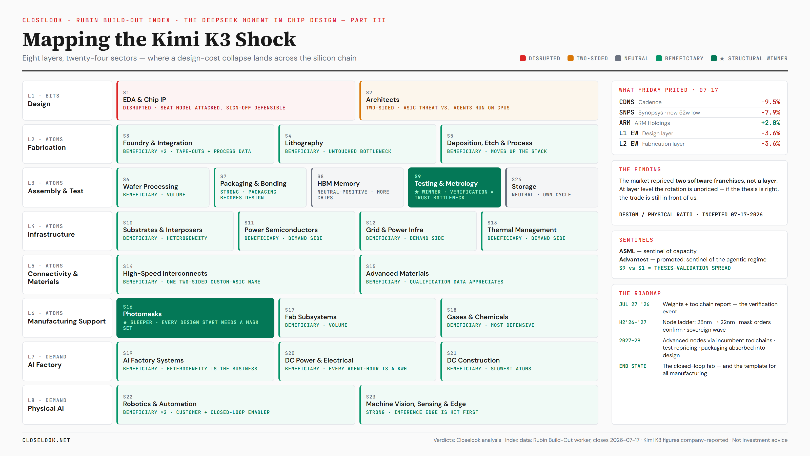
The map: eight layers, twenty-four sectors
The original silicon core of the index is Layers 1 through 6; the v2 extension added Layer 7 (the AI factory) and Layer 8 (physical AI) — and the extension turns out to matter, because several of the sectors added in June are precisely where a design explosion discharges.
Layer 1 — Design. The layer under attack.
S1 EDA & Chip IP — disrupted, with a bifurcation. The seat-based tool business — software operated by scarce human engineers, priced per engineer — is what a 48-hour autonomous flow attacks. What it does not attack, yet, is sign-off: the verification stack foundries actually trust, the certified IP libraries, the decades of PDK relationships. Part II laid out the fork: verification substrate that agents call, or erosion from below. The tell: the first agentic product from either major priced per completed design objective rather than per seat. Inside the same sector, the IP licensors deserve their own line — and Friday drew it for us. More design starts should mean more licenses; that is the case the market voted for when it bid ARM up two percent into the selloff. But an agent that generates simple cores rather than licensing them attacks the royalty model from the bottom of the range — K3's from-scratch compiler is the proof of principle. Advanced IP is safe for years; commodity licensing is the canary.
S2 Architects — two-sided, and the most misunderstood exposure in the index. The bear case: if every hyperscaler, sovereign program, and vehicle platform can field design agents, the custom-ASIC assault on the general-purpose GPU premium accelerates. The bull case is just as mechanical: design agents run on accelerators, and a world of ten thousand 48-hour design runs is a world of more inference demand, not less. Both are true, on different segments — the roadmap section below says which. One constituent sits precisely on the fault line: Broadcom's custom-silicon franchise is the human-powered version of what K3 automates. It sells exactly the engineering labour the agent replaces — while owning the customer interface, the IP, and the advanced-node flows the open-source stack cannot reach. It is simultaneously the disrupted and the harness. Whether its design pipeline expands (agents multiplying its throughput) or compresses (customers internalizing agentic design) is one of the cleanest single-name experiments the thesis will run.
Layer 2 — Fabrication. The first beneficiary tier.
S3 Foundry & Integration — beneficiary, twice over. Design abundance means more tape-outs flowing toward a fixed number of qualified manufacturing ecosystems. And the subtler effect from Part II: as AI enters manufacturing itself, the leading foundry's decades of process and yield data become training data. The first winner of AI-in-manufacturing is the incumbent.
S4 Lithography — untouched and appreciating. No agent generates an EUV source. As designs flood in, the physical bottleneck's scarcity value rises. Nothing about Friday changed a single scanner delivery date.
S5 Deposition, Etch & Process — beneficiary, moving up the stack. Volume, plus the shift already underway: digital twins, virtual silicon, closed-loop process control. Whoever translates designs into yieldable reality collects the toll.
Layer 3 — Assembly & Test. Where the thesis gets specific.
S6 Wafer Processing & Precision — beneficiary. A volume play on design starts, full stop.
S7 Advanced Packaging & Bonding — strong beneficiary. Packaging is absorbed into design — the agent co-optimizes die, memory placement, interconnect, and thermal in one loop. Every custom die the explosion produces still needs bonding, and heterogeneous custom silicon needs more of it, not less.
S8 HBM Memory — neutral to positive. Custom inference silicon may carry less HBM per chip than a flagship GPU — but there are more chips, and the diversity of accelerators still funnels into the same three HBM suppliers. The sector's leadership of the Early Ramp phase this year was Rubin-cycle-driven; K3 does not interrupt it.
S9 Testing & Metrology — the structural winner of the entire thesis. Here is the sentence this essay exists to deliver: when design becomes machine-generated and abundant, verification becomes the trust bottleneck. Somebody has to prove that AI-designed silicon works — at sign-off, at wafer sort, at final test. Test intensity per design rises precisely when the number of designs explodes; no other sector carries that double exposure. In the old regime, our sentinel logic used test as a 9-to-12-month lead indicator on the generation ramp. In the new regime the sector is promoted: it is the sentinel of the agentic transition itself.
S24 Storage — neutral to positive, on its own cycle. More inference and more agents mean more data in motion, but the sector trades on the memory cycle, not on design economics. This week's violence in the storage complex was leverage unwinding in Tokyo and Seoul — orthogonal to K3, and a reminder not to read every red candle through one thesis.
Layer 4 — Infrastructure. The demand-side beneficiaries.
S10 Substrates & Interposers — beneficiary. More heterogeneous designs, more substrates; the coming glass-substrate era compounds it.
S11 Power Semiconductors, S12 Grid & Power, S13 Thermal — beneficiaries on the demand side. A 2.8-trillion-parameter model whose own documentation assumes multi-accelerator deployments, running 48-hour autonomous engineering sessions, is pure incremental load. And as the roadmap section shows, the power layer was binding on the flagship roadmap before anyone in Beijing pressed run.
Layer 5 — Connectivity & Materials.
S14 High-Speed Interconnects — mostly beneficiary, with one constituent — Marvell — carrying the same two-sided custom-silicon exposure flagged for Broadcom in Layer 1: its custom-ASIC franchise sells the labour the agent replaces while owning the interface the agent needs.
S15 Advanced Materials — beneficiary. Once AI searches a much larger process space, it discovers new resists, chemistries, and thermal materials faster — which does not displace materials suppliers; it makes their chemical libraries, production consistency, and qualification data more valuable.
Layer 6 — Manufacturing Support. Home of the non-obvious winner.
S16 Photomasks — the sleeper. Every design start requires a mask set. If the thesis's central prediction is an explosion of design starts, mask demand is its most direct physical expression. And the detail the market has not priced: the explosion arrives at mature nodes first — 45nm, 28nm, 22nm — because that is where open toolchains work today and where sovereign programs can actually fabricate. Mature-node mask making is precisely the business the market had written off as legacy. Watch mask order books as the earliest hard confirmation.
S17 Fab Subsystems & Process Infra — beneficiary. Volume through the equipment chain.
S18 Gases, Chemicals & Consumables — beneficiary, and the most defensive expression. Wafer starts are wafer starts, whoever designed the die.
Layer 7 — The AI Factory. Added in June; the demand side made explicit.
S19 AI Factory Systems — beneficiary. A proliferation of accelerator architectures is a proliferation of integration, validation, and deployment work for the rack-and-system builders. Heterogeneity is their business model.
S20 DC Power & Electrical and S21 DC Construction — beneficiaries, slowest-moving atoms in the chain. Every agent-hour is a kilowatt-hour somewhere. The design explosion runs on the same grid interconnect queues and build timelines that were binding before it started — which is precisely why these sectors sit in the index.
Layer 8 — Physical AI. The receptor sites.
S22 Robotics & Automation — beneficiary, twice. Robot platforms are among the likeliest customers of cheap custom inference silicon — stable workloads, cost-sensitive, volume. And on the longer arc, robotic fabs are the third precondition of the closed-loop factory Part II described. The sector is both a customer of the design explosion and an enabler of its end state.
S23 Machine Vision, Sensing & Edge — strong beneficiary. The design explosion attacks the inference edge first, and the edge is where vision and sensing silicon lives. This sector is also, quietly, the physical half of the verification story: machine vision is how atoms get checked against bits.
Sentinels and the new ratio
Our sentinel doctrine assigned ASML the capacity cycle, Micron the memory cycle, and Advantest the generation ramp. The agentic transition promotes Advantest: if design becomes abundant and trust becomes scarce, test and metrology revenue per design start should inflect before anything else confirms the thesis. ASML remains the sentinel of capacity; Advantest becomes the sentinel of the regime.
Two instruments follow. First, the Design/Physical Ratio — the Design layer against a composite of Fabrication and Assembly & Test — incepted July 17, 2026, published once the geography wrinkle is handled honestly (the physical side is Asia-heavy, so the ratio needs either a like-for-like regional cut or an explicit note that it breathes with the yen and the Nikkei as well as with the thesis). Second, S9 against S1 — Testing & Metrology relative to EDA — as the thesis-validation spread, with the same caveat: S9 is heavily Japanese, and its cleanest reading is on multi-week horizons, not single sessions.
If the thesis is right, the Design/Physical ratio grinds lower over quarters, S9-over-S1 grinds higher, and mask order books confirm from the volume side. If July 27 brings a replication failure, or agentic flows stall at the bottom of the node ladder, both ratios close — and the index will record that too, without editorial assistance.
Rubin, Rubin Ultra, Feynman
The cleanest formulation: Kimi K3 changes nothing about what the flagship architect ships, and a great deal about what ships around it.
Rubin, ramping in the second half of 2026, was design-frozen years ago. Its HBM4 is booked, its packaging capacity allocated. No autonomous design agent touches it. If anything, K3 is incremental demand — agents consume tokens, and the model class K3 represents requires exactly the multi-accelerator infrastructure Rubin exists to provide. The Early Ramp phase of the generation cycle proceeds untouched.
Rubin Ultra, second half of 2027, is likewise beyond design's reach — and its reported turbulence is instructive for the opposite reason. The next-generation rack architecture has reportedly slipped, and the most aggressive multi-die configuration has reportedly been scaled back under customer pushback. Read that carefully: the constraints already binding on the most important product roadmap in technology are power, racks, cooling, and packaging — Layers 4 and 7 of this index — and they were binding before the demonstration. The market spent Friday discovering that the design layer was never the bottleneck. The flagship roadmap had been demonstrating it for months.
Feynman, 2028, is where the two stories intersect. The first generation whose design cycle overlaps with mature agentic design, and two forces pull in opposite directions. The incumbent is not a bystander: it will run design agents internally — it already pushes AI through computational lithography and its EDA partnerships — so Feynman's own iteration loop compresses. The ketchup bottle pours for the defender too. But Feynman also launches into a market with dramatically more custom competition — concentrated, and this is the essential asymmetry, at inference. K3's demonstration chip was an inference accelerator. The design explosion attacks the inference edge first, where workloads are stable enough to justify fixed silicon, while frontier training remains general-purpose — and the incumbent's — for years longer. The generation framework's eventual “architects flatten” phase does not move forward for training silicon. It moves forward materially for the inference share of the market.
What the index does now
Nothing, this week — and that is worth stating plainly, because it is the discipline the structure was built to enforce. The index rebalances on schedule, not on news. An instrument that reacted to every demonstration would measure our own excitement; an instrument of permanent layers with scheduled rebalancing measures the rotation. The same discipline applies one shelf down, in the portfolio books that express the structure: nothing was bought or sold on Friday, and nothing will be because of a launch event. What changes is the lens — the two ratios above, the sentinel promotion, and a watchlist that now reads mask orders and mature-node bookings as thesis data.
That is the point of building the instrument before the event. DeepSeek showed that intelligence could be reproduced cheaply, and the market needed a year to trace the consequences. Kimi K3 claims intelligence can now design its own silicon, and the consequences will trace faster — first through the bottleneck in bits, then, much more slowly and much more valuably, through the world of atoms this index spends six of its eight layers watching.
K3 will not be the only one: the fab is the rehearsal space
One question remains, and it is the one that extends past silicon: why did this happen in chip design first — and where does it happen next?
The answer to the first half is a checklist. Agentic engineering lands earliest where three conditions hold: a hard external verifier (the work is checked by simulators and rule decks, not by opinion), a fully digitized workflow (the entire object of work exists as files a model can read and write), and extreme value density (one design justifies any compute bill). Chip design is the only industrial domain that scores maximum on all three. That is why the first DeepSeek moment for engineering happened at 45 nanometers and not in any other factory.
But walk the checklist across the industrial landscape and a sequence falls out.
Next in line: the rest of engineering software. Structural, fluid, and electromagnetic simulation — the CAE world — has the same shape as EDA: digitized workflows, physics-based verifiers, seat-based pricing operated by scarce specialists. The same fork applies: become the verification substrate agents call, or watch objective-priced agents erode the seat model from below. It is no accident that one EDA major spent heavily to own simulation assets; the agentic question that hit its chip tools on Friday arrives at its physics tools next. The broader PLM and industrial-design complex — the software that defines every manufactured object — follows the same logic on a longer fuse, because its verifiers are softer and its workflows less closed.
Then: process development wherever a digital twin gets good enough. Battery cell engineering, specialty chemicals and advanced materials, biologics process development, precision machining — each is a loop of design, experiment, measurement, and adjustment in which physical trials are the cost and the calendar. Part II's three conditions for the closed-loop fab — valid recipes, predictive twins, robotic execution — are the generic conditions for AI-run manufacturing everywhere. Semiconductors will meet them first, for the same three reasons as always: the fab is the most instrumented factory on earth (in-line metrology at every step is the verifier), its processes are the most simulated (the twin is furthest along), and its economics are the most extreme (a yield point at the leading edge is worth more than most factories). Whoever proves closed-loop autonomous manufacturing in a fab owns the template for the gigafactory, the chemical plant, and the biologics suite.
The investing consequence is a transferable pattern, not a list of names. In every domain the sequence touches, value migrates the same way it is migrating in silicon: away from engineering labor and seat-based tools, toward the reality layer — the instruments that measure, the equipment that executes, the data that only incumbents possess, and the verification authority that certifies machine-generated work. Every industry has an S9. Finding it before the rotation arrives is the exercise; the semiconductor chain is where the answer key is being written first.
This is also why the index's June extension earns its place in this story. Layers 7 and 8 — the AI factory and physical AI — are the receptor sites where the pattern lands: the robots that execute closed loops, the vision systems that verify atoms against bits, the power and construction chains that feed every agent-hour. The taxonomy did not need K3 to justify them. K3 is simply the first event that lights the whole board at once.
The formulation
The baton is changing hands. Design becomes abundant; trust, capacity, and measurement become the scarce assets — first in silicon, then wherever atoms are made to order. We built the camera years ago and pointed it at the exchange zone. Semiconductors are not just the substrate of artificial intelligence. They are the rehearsal space for AI-run manufacturing — and the rest of the industrial economy is the tour.
Watch the fab to see the factory.
Closelook is an investment diary. Nothing here is investment advice or a recommendation to buy or sell any security. Sector and constituent references describe the composition of the Closelook Rubin Build-Out index framework. All Kimi K3 performance figures are company-reported pending the July 27 weights release and technical report. Index figures reflect Rubin Build-Out worker data at the July 17, 2026 close.