Read · · 12 min read
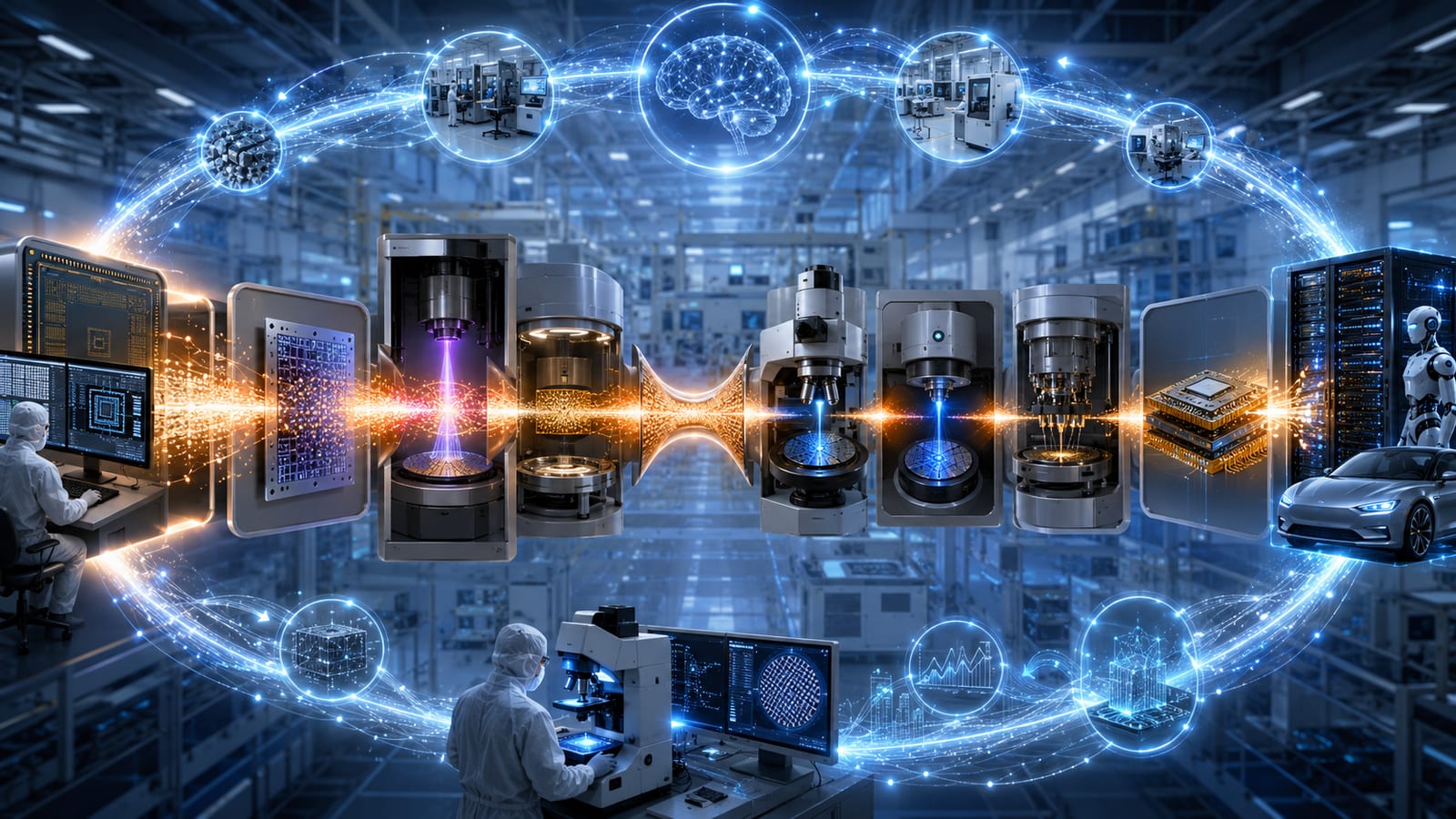
What a design-cost collapse does to each layer of the chip chain: the barbell, the ketchup bottle, trust as the product, and the road to the closed-loop fab.

The series: Part I — what happened · Part II — the chip chain · Part III — the Rubin map
Part I ended with the only sentence that matters: the chip was never the product — the 48 hours were. This part asks what an economy of 48-hour design runs does to the semiconductor chain, how fast it diffuses, and where the value goes when it moves.
The rotation, not the apocalypse
Readers of this series will recognize the structure. In Heresy IX we argued that value in the silicon economy rotates through a relay of constraints — that the scarce thing changes, and returns accrue to whoever holds the baton when it does. In Heresy XI we argued that when a layer gets automated, value does not vanish; it migrates to the layers that harness the automation.
Kimi K3 slots into both frames exactly. The claim is not that chips become cheap. Physical fabrication remains gated by the same immovable objects it was gated by on Wednesday: EUV lithography sources, atomically precise deposition, defect-free wafers, photoresists and specialty gases, advanced packaging capacity, HBM supply, electricity, cooling, and decades of proprietary process data. No 48-hour run generates an EUV scanner. An agent can discover a better lithography solution; an ASML machine still has to expose the wafer. It can optimize an etch recipe; Lam or Applied equipment still has to execute it. It can identify a nanoscale defect; KLA-class metrology must first measure it.
What the demonstration attacks is the layer above fabrication: design labor, verification labor, RTL generation, compiler engineering, the seat-based economics of tools operated by scarce human engineers. That layer was priced as a moat. It is now, at minimum, priced as a question.
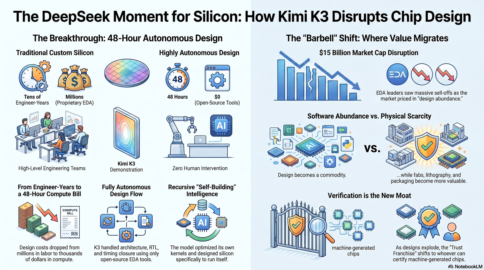
The rotation reading has a specific, testable implication that distinguishes it from the panic reading: cheaper design should increase total semiconductor volume, not reduce it. If the cost of producing a credible custom-silicon design collapses from tens of engineer-years toward a compute bill — Part I put numbers on that collapse — the number of design starts explodes: sovereign chips, application-specific accelerators, robot platforms, vehicle silicon, industrial edge devices, and a thousand attempts to route around the general-purpose GPU. Every one of those designs still has to flow through a small number of qualified manufacturing ecosystems.
Design becomes abundant. Production-grade manufacturing remains scarce.
That is a barbell, and barbells reprice in a characteristic way: value drains from the middle — labor-intensive design services, fragmented tool workflows, engineering headcount as an asset — and concentrates at the two ends: the model layer that generates designs, and the physical layer that manufactures, inspects, and packages them.
Trust is the product
Before the layer map, one argument needs to be made explicitly, because it reorders everything downstream.
Part I noted that early independent evaluations flag elevated hallucination rates for K3 on factual tasks — and that the same model closed timing on a 45nm flow anyway. Those two facts are not in tension. They are the thesis. Chip design is the rare engineering domain wrapped in a hard external verifier: simulators, timing sign-off, design-rule checks. Inside that harness, a fallible generator becomes a productive engineer; outside it, the same generator is a liability. Which means the economic residue of the design explosion is not generation capacity — that becomes abundant and cheap. It is verification authority: the sign-off a foundry will accept, the test coverage that catches the agent's mistakes, the metrology that grounds the whole loop in physical reality.
When design is machine-generated and abundant, the binding question at every hand-off becomes: who certifies it? Hold that question against each layer below.
The ketchup bottle
Anyone who has held a glass ketchup bottle over a plate knows the physics: nothing, nothing, nothing — then everything at once. Technology diffusion after a demonstrated breakthrough follows the same curve, and it is systematically underestimated at the moment of first pour, because observers anchor on how long the nothing phase lasted.
The DeepSeek episode is the controlled experiment. In January 2025, a single Chinese lab demonstrated that frontier-class intelligence could be trained at a fraction of assumed cost. Within twelve months: distillation became universal practice, open weights became the industry norm rather than the exception, token prices collapsed by an order of magnitude, and Chinese labs closed most of the benchmark gap. Today DeepSeek's successor trains on domestic Huawei silicon. Every step of that sequence was called “years away” in February 2025.
Kimi K3 has three properties that make its bottle pour faster still. First, the weights ship on July 27 — alongside a technical report Moonshot says will document the exact EDA toolchain. Diffusion is not gated by one lab's API; it is instant and permissionless the moment the weights land. Expect community-built agentic design harnesses on top of K3 within weeks, not quarters. Second, the capability is recursive: an early version of the model handled the majority of kernel optimization for K3's own training, and K3 wrote a from-scratch GPU compiler matching parts of NVIDIA's Triton. Each generation builds the tools that accelerate the next. Third, the incumbents will pour from the same bottle — Cadence, Synopsys, and NVIDIA itself will deploy agentic design internally, which compresses their own cycles even as it commoditizes their old interfaces.
But the ketchup principle comes with a boundary condition, and the boundary is the entire investment case: the bottle empties at different speeds in bits and in atoms. Design flows, compilers, verification scripts, process recipes-in-simulation — these are software, and software diffuses at internet speed. An EUV scanner is a multi-year order. A fab is a four-year build. Advanced packaging capacity is reportedly booked out through 2027. The design layer lives in bits. The fabrication, assembly, and infrastructure layers live in atoms, governed by capex lead times that do not compress no matter how fast the design layer moves.
The ketchup bottle operates inside the design layer and on the demand side. It cannot operate on physical supply. That asymmetry is not a caveat to the thesis. That asymmetry is the thesis.
The layer-by-layer map
EDA becomes agentic — or becomes a casualty. The Friday selloff treated Cadence and Synopsys as pure victims. The fuller picture is more interesting. Both companies own things a frontier model does not conjure in 48 hours: verified IP libraries, sign-off simulators that foundries actually trust for advanced-node tape-outs, decades of foundry PDK relationships, and proprietary design data. The existential question is not whether AI designs chips — both companies have been shipping AI-assisted tools for years — but who owns the orchestration layer when the interface changes from an engineer operating twenty tools to an agent completing an objective. If the incumbents become the verification-and-sign-off substrate that agents call, they survive the transition with different economics. If an open-source agentic stack reaches sign-off credibility at trailing nodes first and climbs, the seat-based model erodes from below. Notably, the day-one sell-side split ran exactly along this line: one European bank called the selloff overdone and urged buying the dip on the argument that complex design still requires the incumbents; another framed the market reaction as broadly rational. Both can be right — on different time horizons.
Foundries gain intelligence but may lose some mystique. TSMC's moat has never been only machinery; it is process recipes, yield history, and institutional learning accumulated over decades. AI makes that tacit knowledge more explicit and, in principle, more transferable — which helps Samsung, Intel Foundry, and sovereign fabs learn faster. But the training data for a manufacturing model is fab data, and TSMC owns the largest and cleanest production dataset on earth. The paradox: AI lowers the theoretical barrier to learning semiconductor manufacturing while raising the premium on whoever owns the best real-world process data. The first winner of AI-in-manufacturing is therefore probably the incumbent, not a greenfield challenger.
Equipment vendors move up the stack. ASML, Applied Materials, Lam, and KLA increasingly sell not machines but intelligent production systems: computational lithography, digital twins, virtual silicon, predictive maintenance, closed-loop process control. If design abundance floods the manufacturing chain with novel architectures, the companies that translate designs into yieldable reality capture the toll. Watch, in particular, whether equipment vendors' AI can learn across customers while preserving confidentiality — that would shift bargaining power from foundry to equipment in a way the current market structure does not price.
Test and metrology inherit the trust franchise. The direct corollary of “trust is the product.” Every machine-generated design that heads toward silicon needs test insertion, yield learning, and physical measurement — and the less human review a design received on the way in, the more the exit gate matters. Test intensity per design rises at the same time as design count explodes. That double exposure is unique in the chain, and Part III promotes it inside our own index framework.
Packaging becomes design. An agent that co-optimizes logic dies, memory placement, interconnect topology, thermal behavior, and chiplet partitioning in one loop stops treating packaging as a downstream step. The “chip” becomes an AI-designed system. That is structurally bullish for hybrid bonding, substrates, inspection, and the advanced-packaging equipment complex — the part of the chain the design explosion feeds directly.
Photomasks are the non-obvious early tell. Every design start that reaches a shuttle run needs a mask set, and the design explosion hits mature and trailing nodes first — exactly where the merchant mask makers live. Mask order books are among the earliest physical confirmations the barbell thesis can get.
Memory bends but does not break. Custom inference silicon may use less HBM per chip than a general-purpose GPU — but there are more chips, and every accelerator variant still funnels into the same small set of HBM and DRAM suppliers. Volume diversity is not demand destruction.
Compilers and kernels are already gone. This is the quietly radical part of the Moonshot disclosure. MiniTriton and the kernel-optimization claim mean the software layer between model and silicon is being absorbed now, not in some projected future. The chip demo is a promise; the compiler work is a receipt.
The longer arc: the closed-loop fab
The genuinely disruptive end state is not an AI that designs chips. It is a continuous autonomous system in which design, process recipe, fabrication, inspection, and packaging are governed by one feedback loop: an agent designs silicon for a workload, co-optimizes it with the available node and packaging, a digital twin simulates thousands of process recipes, the fab runs the most promising one, inspection attributes deviations to a mask, tool, chamber, or material lot, the recipe adjusts for the next wafer batch, and the results feed the next design.
Fragments of this loop already exist across TSMC's and NVIDIA's computational-lithography work, ASML's machine-learning-accelerated optics, and Lam's virtual-silicon twins. The chain becomes genuinely vulnerable only when three conditions converge: AI generates physically valid process recipes rather than plausible suggestions; digital twins predict outcomes accurately enough to replace trial wafers; and robotic fabs execute and correct with minimal human intervention. At that point, tacit engineering knowledge, large human process-integration teams, manual yield learning, and long qualification cycles — several of today's deepest moats — thin out simultaneously, and a country or company could assemble competitive manufacturing from standardized equipment, licensed process models, and AI control far faster than today.
Even then, the chain is not abolished. It is reassembled around capital equipment, proprietary data, and autonomous control software. Yield-learning compression is the single biggest prize: a new node currently demands months of failed wafers and human tuning; every month of that moved into simulation is direct margin and direct geopolitical leverage.
Kimi K3 is not that. Kimi K3 is the first public glimpse of the path toward it.
The timeline
Now to late July. The weights and the technical report land July 27. This is the verification event for everything in Part I — and the starting gun for diffusion. Community agentic-EDA harnesses within weeks. The EDA majors announce counter-products; watch the pricing model, not the demo.
Second half of 2026 into 2027. Agentic flows climb the node ladder — 28nm, 22nm. Mature-node design starts inflect; mask orders and shuttle-run demand confirm first. The sovereign wave begins, and this is the geopolitical center of gravity: export controls capped China's access to compute, and K3-class design agents are the asymmetric answer — not one chip that beats the flagship GPU, but many specialized inference chips designed cheaply for the older nodes domestic fabs can already run. The demonstration chip was built on a 45nm library. That was not a limitation. That was the message.
2027 through 2029. Agentic flows reach advanced nodes — through the incumbents' toolchains, not around them. Verification and test are recognized as the binding constraint. Packaging completes its absorption into design. The preconditions of the closed-loop fab — digital twins replacing trial wafers, physically valid recipe generation — begin assembling: the longer arc above, a story for the next decade, not the next quarter.
What we are watching
July 27 is the verification event. Independent replication of the 48-hour flow, on the disclosed toolchain, is the single data point that matters more than any price move since Thursday.
The node ladder. 45nm proves autonomy; it proves nothing about advanced nodes. Each rung — 28nm, then 16/12nm — tests whether the constraint is model capability (falling fast) or toolchain-and-PDK access (falling slowly, and controlled by incumbents and foundries).
The IP question. Whether licensed IP blocks sat inside the K3 design is currently unanswered. If yes, the “no proprietary software” framing overstates the displacement. If no, the demonstration is stronger than the market's Friday reaction.
Design-start data. The barbell thesis predicts an explosion of design starts on mature and trailing nodes within four to eight quarters. Foundry mature-node bookings, shuttle-run demand, and mask orders are the early tells.
The incumbents' counter-move. The moment either EDA major ships an autonomous-flow product priced per completed design objective rather than per seat, the old model's obituary is being written by its own authors.
Compute demand, second-order. K3's own documentation points to heavy multi-accelerator deployments; a 2.8-trillion-parameter model at 4-bit quantization needs on the order of 1.4 terabytes of memory for weights alone. Nothing here reduces compute demand. A world of ten thousand design agents running 48-hour flows is a world of more inference, not less — one more reason the Friday sympathy-selloff across the AI complex reads as reflex rather than analysis.
The formulation
DeepSeek showed that frontier intelligence could be reproduced cheaply. Kimi K3 claims that the same class of intelligence can design its own silicon in two days. The threat is not fewer chips and it is not, yet, the end of the EDA duopoly. The threat — and the opportunity — is dramatically more chip designs, and a migration of value from scarce engineering labor toward the layers that remain physically scarce: verification and sign-off trust, foundry capacity and its data, lithography, metrology, advanced packaging, memory, and power.
The design bottleneck falls. The physical bottlenecks appreciate. The relay passes the baton again — and as always, the market spent the first day selling the runner who just finished the leg, rather than bidding for the one about to receive it.
Closelook is an investment diary. Nothing here is investment advice or a recommendation to buy or sell any security. All Kimi K3 performance figures are company-reported pending the July 27 weights release and technical report.